Development and application of matrix CCD sensors and CMOS sensors
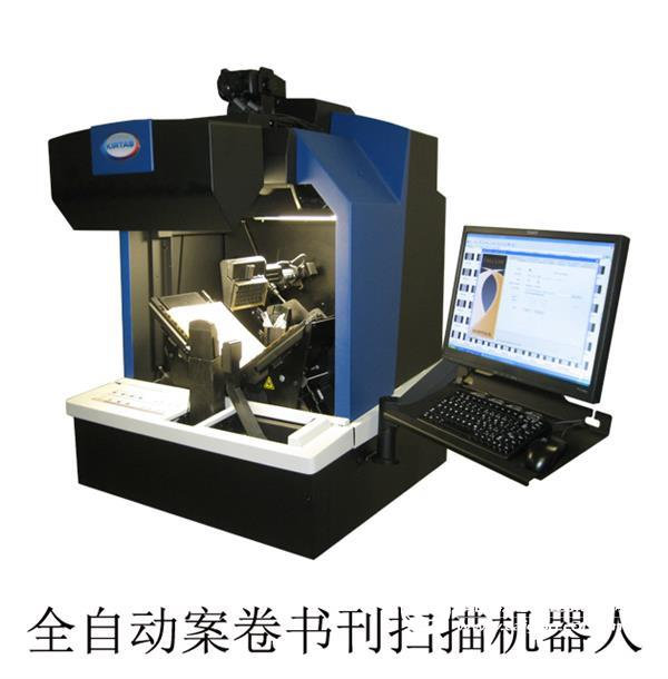
The sensor is one of the core components of a book scanner. The image sensor of the scanner basically used linear CCD in the early years. Most of the early image acquisition devices used this imaging technology, such as copiers, flatbed scanners, paper-fed scanners, large-format scanners, and so on. With the development of sensor technology and the refinement of image acquisition equipment, the use of sensors is also very different. The CIS processor is the cheapest, low-end flat-panel, entry-level paper-fed scanners are often used with contact image sensors CIS (or LIDE); relatively low-cost linear CCD or CMOS sensors are used in low-end book scanners, entry Grade non-contact scanners, large format scanners, copiers, etc.; higher-priced aerospace-class matrix CCD sensors are used in aerospace, simulation and replication, top-level book scanners, non-contact file scanners, etc. . There are many arguments in the jar about the question of matrix CCD and CMOS, linear CCD, and CIS. For the majority of users, this is a good thing.
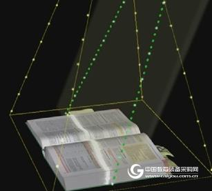
First of all, the function of the image sensor is to convert the light energy into an electrical signal and digitize it to form a digital image. Whether it is implemented in matrix CCD technology or linear CCD, CMOS, CIS imaging technology, this function is completed. Because cis imaging technology is mostly applied to low-end image acquisition devices, we will not introduce them here. Below we mainly introduce the matrix CCD technology used in the book scanner or the linear CCD and CMOS.
The two terms of CCD and CMOS are not specifically referred to as image sensors, but are generic terms for both semiconductor technologies. A CCD (Charge Coupled Device) is translated into a "charge coupled device", and a CMOS (Complementary Metal Oxide Semiconductor) is translated into a "complementary metal oxide semiconductor." Whether it is CCD or CMOS, most of the photoelectric conversion is to form a "photodiode" on the semiconductor by utilizing the characteristics of silicon. (Of course, there are also CCDs that use polysilicon polysilicon). This is the same principle as solar cells.
Both CCD and CMOS technologies were formed in the late 1960s and early 1970s. The original intention of the invention of the CCD was to perform data storage. But this feature was completely replaced by later CMOS and magnetic media. However, the CCD did not die, but it shined in image recording. Since the 1970s, CCDs have been used in products such as video recorders. In the 1980s, CCD began to be used by the earliest digital cameras. Many of the shortcomings of CCD sensors that affect image quality have been overcome one by one. In the 1990s, CCD was used in the field of image scanning. For 30 years, CCD image sensors have been fully mature.
Then we start from the CCD technology, the CCD is to convert the light energy signal into electric charge by the photosensitive array, then “transfer†the charge to the unified circuit line by line, convert it into voltage signal, send out the sensor chip, and output to independent. On the analog to digital converter ADC. The ADC then passes the converted digital image signal to the camera's image processor.
The advantages of the CCD book scanner are: simple sensor design, high sensitivity, excellent image quality and mature technology.
But CCD technology is not without its drawbacks. In summary, there are several problems:
1) The biggest problem is the cost of production. Since linear CCDs cannot use mainstream CMOS lines, and production is not so large, production costs cannot be reduced on a large scale. This problem is still difficult to solve.
2) Linear CCD sensors require additional ADC, amplifier, and other support modules to be used. In this way, one increases the development and manufacturing costs; the other is that excessive analog circuitry outside the chip introduces noise, which in turn affects image quality.
3) Reading speed. Since all charges are converted and output through a unified circuit, the reading speed of the linear CCD sensor is relatively slow. Of course, the new generation of matrix CCDs has improved in this respect.
4) Linear CCD charge fading problem. Since the charge acquired in the linear CCD is output line by line in a manner that the coupling shift (which is also the source of the name CCD), the charge is attenuated during the output. This causes image noise.
5) Poor durability, the traditional linear CCD scanning method has great requirements on the durability of the transmission mechanism.
6) Linear CCD relies heavily on the light source, and it needs to be used with high-intensity line lights in the application of the scanner.
These are probably the weaknesses of CCD. Although the manufacturer has overcome it in various ways, the problem has not been completely solved for a long time. Until the emergence of matrix CCD technology, the shortage of linear CCD was completely solved.
Let's take a look at CMOS technology. The reason why today's computer technology is so developed is, in the final analysis, due to advances in semiconductor technology, especially CMOS technology. The CPU, memory, flash memory and many other devices we use are all CMOS technology. Simply put, the advantages of CMOS are high integration, low production costs, and power savings.
On the surface, the construction of CMOS sensors and CCD sensors is very similar. The photosensitive array converts the optical signal into an electrical signal and then outputs it through a CMOS circuit. However, there are a few big differences:
1) CMOS is equipped with a signal amplifier and other supporting circuits at each photosensitive point of the photosensitive array. The advantage of this is to improve the anti-interference ability of the signal. There are two disadvantages: one will form "Fixed Pattern Noise" (FPN. I will talk about it later); the second is that these amplifiers and support circuits will occupy The light energy receiving area reduces the receiving sensitivity of the sensor.
2) Modern CMOS sensors integrate the analog-to-digital conversion circuit ADC and other supporting circuits on the chip. The development difficulty and manufacturing cost of the system are reduced, and the reliability is improved.
3) CMOS uses a single supply, single reference voltage. Reduces power consumption, improves system reliability, and reduces noise interference generated by peripheral circuits.
In simple terms, CMOS sensors effectively solve or improve the shortcomings of the CCDs mentioned above. Of course, the most important one is to greatly reduce production costs.
So what are the disadvantages of CMOS?
CMOS has two biggest drawbacks to overcome:
1) Fixed mode noise FPN. As mentioned earlier, in a CMOS sensor, each sensor has a signal amplifier and other support circuits. However, in the production process of semiconductors, the gain and bandwidth of each amplifier formed are different, so the two pixels of the same brightness will have different values. From the whole picture, there will be a "fixed noise picture". For example, an 18% grayscale picture, the final brightness is not the same everywhere.
But since the noise pattern is "fixed", there is a way to solve it. The most effective way is the so-called "double sampling". That is, after the camera shutter is closed, the image is read out for 10 milliseconds, then the sensor is reset, and then the second sampling is performed for 10 milliseconds to obtain a noise pattern. By subtracting the noise image from the original image, the fixed pattern noise can be effectively eliminated. This method is especially effective for eliminating the fixed pattern noise of the camera. Of course, if it is a camera, it will be more complicated.
2) The second big problem with CMOS sensors is that the sensitivity is not as good as the CCD sensor. For CCDs, the entire sensor area can be used to receive optical signals. The fill factor can approach 100%. However, for CMOS sensors, since each area of ​​the photosensitive array requires a part of the area to be used as a signal amplifier and a supporting circuit, the photodiode cannot be made large. The light-receiving rate (as if the word "opening rate" is commonly used) is much less than 100%. A few years ago, CMOS's light-receiving rate was only 20%. This will greatly reduce the sensitivity of the sensor.
3) The application of CMOS sensors on scanning devices is not mature enough, and related accessories and image processing are not perfect.
There are two ways to solve the low sensitivity of CMOS sensors: First, with the development of semiconductor technology, the line width of CMOS is getting smaller and smaller, and more and more circuits can be done in the same area. Or, the same circuit, the required area is getting smaller and smaller. This leaves the area of ​​the photosensitive circuit larger and larger, and the ratio is getting higher and higher. With the rapid development of CMOS technology, the light receiving rate will be further improved; the second is to use "Micro Lens" to polymerize the light energy at one pixel to the "opening" position of the photodiode.
Through the above introduction we have seen that CCD technology is fully mature, and CMOS technology is still in progress. But in terms of image quality, today they are already comparable. Even some differences are insignificant compared to the backend image processor.
After more than 30 years of development, the CCD sensor has matured. However, there are still three major problems to be solved: high production costs, poor system integration, and power consumption.
CMOS sensors can solve these three major problems with CCD sensors. But I also have two new problems: fixed mode noise, low sensitivity. Among them, fixed mode noise has been basically solved by the prior art. The sensitivity issue is improving and will continue to improve. At present, the global demand for CMOS sensors is about 9 billion chips per year (2016). With the further expansion of market demand, the rapid development of CMOS sensor technology has been promoted. It is believed that in the near future, CMOS sensors will replace the CCD sensors. At present, the leading manufacturer of CCD processor, represented by Sony, also announced in 2015 that it will officially stop the development and production of linear CCD products in 2017, and fully invest in the development and production of next-generation matrix CCD and CMOS sensors.
Pet Mat,Pet Heating Pad,Portable Pet Pad,Luxury Pet Dog Bed
Yangzhou Pet's Products CO.,LTD , https://www.pqpets.com